
Rev1 Assembly Notes

Debug board

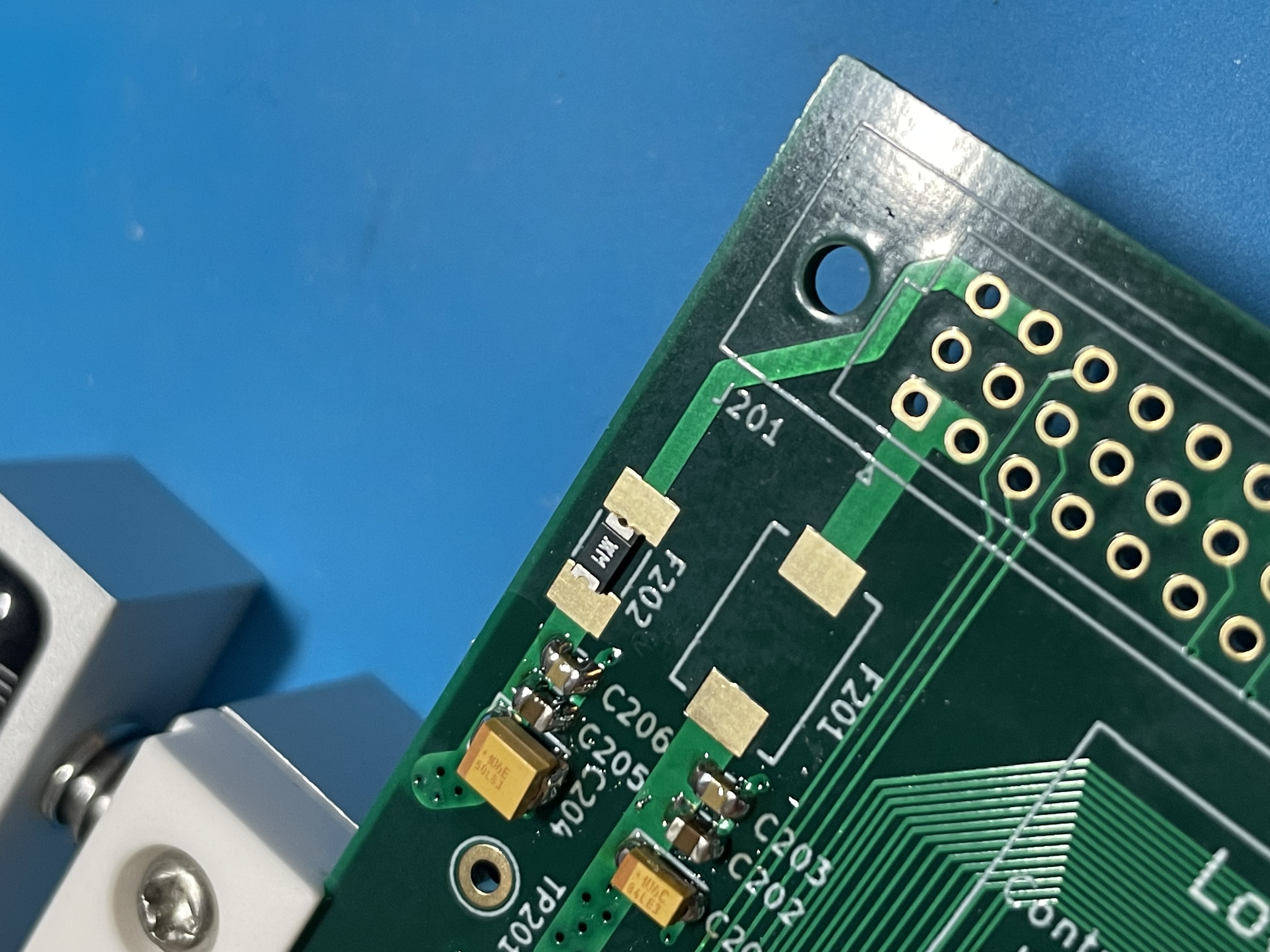
  • F202 footprint appears to be too large for the fuse ordered (NANOSMDC050F/13.2-2)4C4B7710-7F08-4D19-BEB5-0A50049FE9E9.jpeg
  • F201 is actually 1.1A, not 1.5A as the schematics indicate 
  • Caps under Teensy (C316/C317) could use with being moved a bit
  • U508/U509 package sucks ass
  • C512/C511 should be further away from IC in -Y
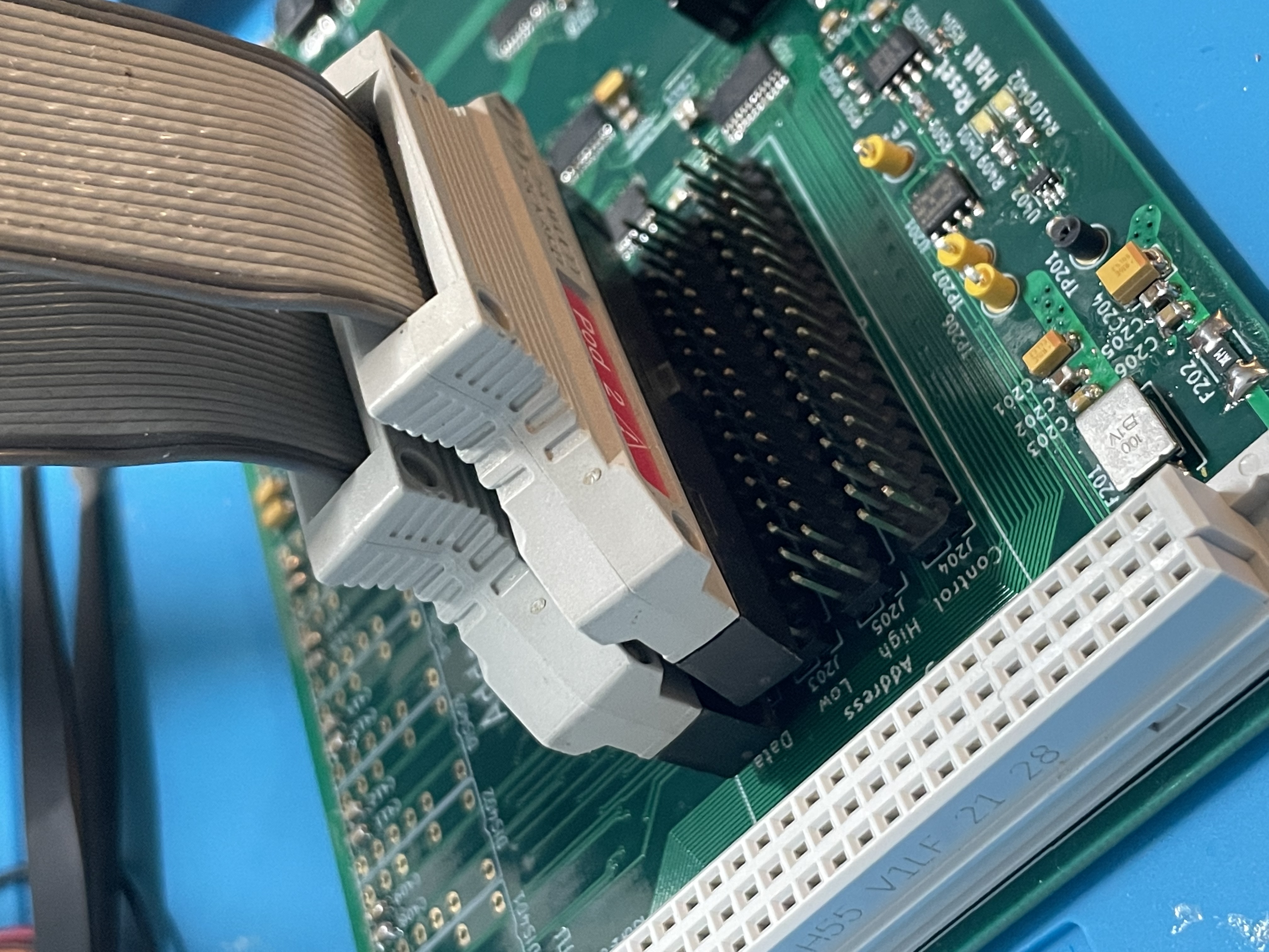
  • The indications for RESET and HALT are inverted (D401, D402) from what they should be
  • Teensy USB port interferes with J302 with some USB cables
  • Solder pads for DIN connectors could be slightly wider copper
  • Logic probe connectors need more spacing in Y direction to fit the probes

D9EAACE4-419B-4D2A-88FB-B2A40D43B003.jpeg

CPU Board

  • +12V fuse (F202) footprint is wrong
  • Reset and NMI button logic is inverted from what it should be (lol)
    • U501 shouldn't be inverting type (use 74HC2G17 instead)
  • D201 should be further set back (.3mm) from board edge
    • The H100 series LED seems to have a slightly different pin-to-front distance than the H201 double LED indicators
  • 5V Analog caps (C608, C609, C614) should be up more
  • LED current limiting resistors are out of whack
    • Lower the current limiting resistors for right angle LED indicators (needs more current)
    • Increase the current limiting resistors for two bonus debug LEDs (needs less current)
  • Read/modify/write cycles may not work right
    • We need to deassert /DTACK when both /LDS and /UDS get deasserted
      • Neither of the byte strobes are on U102, which is responsible for generating /DTACK
      • May be able to bodge these into the GAL, since there’s a few spare inputs
    • Also, the /BERR timer and peripheral waitstate generator are reset by /AS
      • Probably a non issue since RAM is going to be 0 waitstate, and we can say CPU board peripherals don’t support read-modify-write (maybe only an issue for NVRAM)
  • UART B (J503) should be centered between LEDs and UART A jack