If desired, the driver communication interface can use CAN0 instead. It uses the same IO pins as the I²C bus, and requires a CAN transceiver on the board.
# DMA Channel Allocations DMAC should operate with dynamic, round-robin priority arbitration within a DMA priority level. Priority levels listed are from 0 (highest) to 3 (lowest.) - Ch0: NOR flash SPI Tx empty (SERCOM5) - Priority: 2 - Operate in SPI 32 bit data mode - Burst transfers - Ch1: NOR flash SPI Rx complete (SERCOM5) - Priority: 2 - Operate in SPI 32 bit data mode - Burst transfers - Ch2: Display SPI Tx empty (SERCOM4) - Priority: 1 - Operate in SPI 32 bit data mode - Burst transfers # Clocking ### Clock Inputs All clocks on the system are derived from one of the following clock inputs (oscillators and internal generators:) #### Crystals - XOSC1: External 12MHz oscillator - Provides primary system clock reference - XOSC32K: External 32.768kHz oscillator - Runs in standby for RTC #### FLLs - DFLL48M: 48MHz - Used for USB reference clk - Uses external 32kHz osc for reference #### PLLs - DPLL0: 120MHz - CPU core clock ### Clock Sources The above clock inputs are then synthesized into multiple clock sources, each used by a different set of peripherals: - GCLK0: 120MHz - Sourced from DPLL0 / 1 - General high speed clock - GCLK1: 48MHz - Sourced from DFLL48M - Intended for USB use - GCLK3: 32.768kHz - Sourced from XOSC32K - SERCOM slow clock - GCLK4: 12MHz - Sourced from XOSC1 - General low speed clock - GCLK5: 32.768kHz - Sourced from ultra low power 32kHz osc ### Clock Consumers - CPU core: GCLK0 - Clock division factor: /1 - Low power clock: /4 - Backup domain: /8 - High-speed: /1 # Hardware Errata This page lists some issues with CPU board hardware, as they are discovered, and some workarounds. ## Rev 1 - /I2C\_IRQ's external IRQ line conflicts with ENCODER\_A - Move /I2C\_IRQ from PA7 to PA10 - Rework required: solder line from pin 11 (/IRQ) of U101 to middle of J302 (TXD) - Status LED (D302) footprint is wrong - The common (+) and red pins are swapped - Footprint for MMBT3904 transistors (Q101, Q301) are slightly too small - The two pads side is slightly too much spacing between pads - They are still solderable, it just looks ugly - NOR Flash (U303) is actually 4Mbit - This is the part I actually had lol - Power LED driver doesn't work - The weird trick with the two resistors doesn't seem to work… like, at all - We'll have to revisit how this is controlled (external logic? sacrificing another pin?) - Footprint notes - Copper size on the pads could be increased - For mechanical retention of the switch, nudge the outer (switch) pads in by a small amount - Switched front/rear I²C bus (from mux to MCU) is missing pull ups - Need to insert these between the mux (U101) and microcontroller - Rework required: Bodge in a pair of 2k2 resistors to +3V3[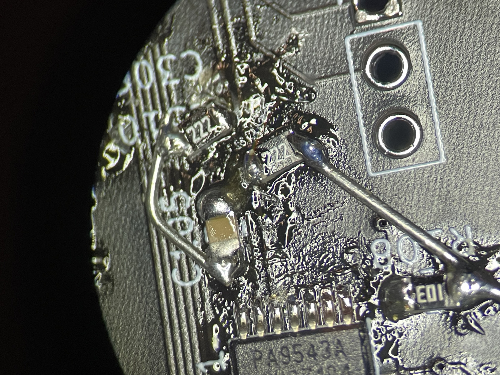](https://wiki.trist.network/uploads/images/gallery/2022-03/GvJv1sbX1ImjcXRK-image-1648709305027.jpeg) # IO Front and rear panels # Front Panel The front panel features a few buttons, indicators, and a rotary encoder. ## Overview [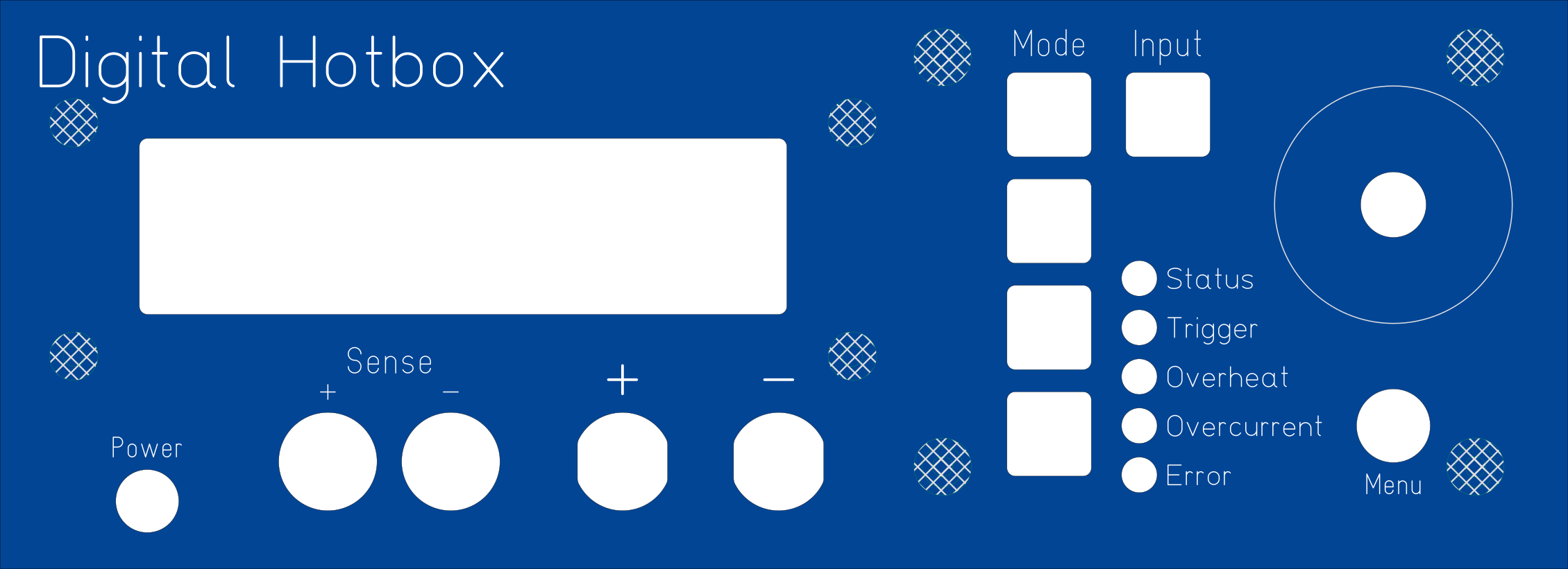](https://wiki.trist.network/uploads/images/gallery/2022-03/EL93mLo1qQbhIc01-image-1647139758326.png) Note that the actual front panel board only covers the right third of the actual front panel: the area with the push buttons, indicators, and rotary encoder. It's mounted to the case via four 8mm standoffs with M2.5 thread, and should be screwed in with washers to distribute the force of button pushes more evenly across the board, rather than stressing the screw holes. ### Connectors There are two primary connections to the rest of the world on the front panel: the external voltage sense input, and the supply input.External voltage sense may or may not be used for measurement, depending on software control.
Supply input is made through a pair of binding posts ([Cal Test CT4231](https://app.caltestelectronics.com/product-list/product-page/view/CT4231/)) supporting up to 36A per post. The positive and negative terminals follow the standard red/black convention, and are internally connected to the driver board via thick wiring. The binding posts should use some sort of screw mount for the wire, which itself should have crimped ferrules or other terminals on the end to attach conveniently to the wire. External sense voltage is delivered through a pair of banana jacks ([Cal Test CT2240](https://app.caltestelectronics.com/product-list/product-page/view/CT2240/).) These do not need to carry much current (if any) and are on a yellow and black connector (for positive and negative, respectively) there. These jacks are solder mount, which should be soldered to a (possibly shielded) twisted pair wire, which in turn connects to the driver board's external voltage sense input. ### Buttons The bulk of the buttons on the front panel consists of illuminated tactile switches ([Omron B3W-9](https://components.omron.com/us-en/products/switches/B3W-9) type), which are further subdivided into the mode selectors (column of four switches, each with a single yellow LED) and the input on/off button (one switch, with dual red/green LEDs.) Additionally, the button inside the rotary encoder (triggered when the knob is depressed) is available as a switch for selecting items in menu. It works in conjunction with the circular menu button ([C&K D6R](https://www.ckswitches.com/products/switches/product-details/Keyswitch/D6/D6RLGN%20F1%20LFS/) type) to browse menus. On the front panel, all buttons are connected to a [XRA1203](https://www.maxlinear.com/product/interface/bridges/gpio-expanders/i2c-gpio-expanders/xra1203) I²C IO expander. It features an interrupt output, which is connected to the controller board so buttons needn't be polled in software. Lastly, there is a power button in the lower left corner; this switch actually exists on the controller board, rather than the front panel. It's an illuminated, right angle tactile switch ([CTS 228A](https://www.ctscorp.com/wp-content/uploads/228A.pdf) type) with the appropriate power icon (the little circle with the dash on it) printed on its cap. The board is set up to support bi-color illuminated switches so that there can be a standby/active type lighting situation. ### Indicators Indicators are LEDs, which are brought out to the front panel via light pipes. These indicators consist of one RGB LED (status,) one amber LED (trigger,) and three red LEDs (overheat, overcurrent, error.) Each LED can be individually controlled, and its brightness (current) adjusted. Each of the buttons, with the exception of the rotary encoder itself, contains at least one LED. These LEDs are available to drive the same way indicators are, via the LED controller. All LEDs are connected to a [PCA9955B](https://www.nxp.com/products/power-management/lighting-driver-and-controller-ics/ic-led-controllers/16-channel-fm-plus-ic-bus-57-ma-20-v-constant-current-led-driver:PCA9955BTW) constant current LED driver. ### Display Any SPI display is compatible with the front panel, though it is specifically designed for the [ER-OLEDM032-1Y](https://www.buydisplay.com/yellow-3-2-inch-arduino-raspberry-pi-oled-display-module-256x64-spi) module (or any other compatible modules with other colors; do note that the display may need to be modified for 4 wire SPI operation, by soldering some resistors and jumpers) and its pinout.Regardless of the type of display, it should not consume more than roughly 350mA of current. The main board has a 500mA polyfuse for the display.
The display mounts on 6mm long M2.5 studs, with nylon stand-offs to get the correct distance between the front panel and the display surface. Then, a washer and nut are attached to the end, to fasten the display securely. ### Miscellaneous On the front panel board, there is also an I2C EEPROM (AT24CS32 type) that contains the front panel’s exact configuration, including the switches available, mapping of switch inputs and LED outputs, and LED drive characteristics such as maximum current. ## Revisions Currently, there’s just one revision of front panel, pictured above. It works, but it needs some minor rework: - Menu button too small: needs +.4mm to diameter - Edge machining on display cutout: A bevel would be more attractive # Rear Panel On the rear of the device are a few auxiliary connections, including AC power input, communications (Ethernet, USB) and an external trigger input. [](https://wiki.trist.network/uploads/images/gallery/2022-03/oUjVicTsUHWcX8G9-image-1647200673543.png) *Rear panel, as viewed from front (inside)* ### Power A cutout is provided for an IEC mains filter/input module with switch and fuse – in this case, the cutout is sized to fit the Astrodyne TDI 084 series, specifically the [084.00301.00](https://store.astrodynetdi.com/filtered-power-entry-modules-with-double-fuse-holder-and-switch084-00301-00.html) with a 3A fuse.It's very important that the IEC input module has a fuse built in; the only protection, if using the driver board's AC/DC module is a varistor to arrest surges.
Output from the filter (usually provided on spade terminals, or directly on wires) should then go via (sufficiently insulated) wires to a connector ([CUI Devices TBP02P1W-381](https://www.cuidevices.com/product/interconnect/connectors/terminal-blocks/tbp02p1w-381-series)-03 or similar 3.81mm pluggable terminal block) to the driver board, which has a power module ([CUI PSK-20D-12](https://www.cui.com/product/internal-ac-dc-power-supplies/board-mount/psk-20d-series/psk-20d-12), [Meanwell IRM-20-12](https://www.meanwellusa.com/webapp/product/search.aspx?prod=IRM-20), or similar) to produce the 12V from mains input. Alternatively, this power module can be skipped in favor of an externally mounted power supply, in which case the mains input can be directly wired there; though take care to ensure that the case is still grounded. (The driver board has a 3.96mm JST-VH B2P-VH connector as a +12V input to accommodate external power supplies in place of a soldered power module, if that is desired instead.) If an external supply is used, it should be capable of providing at least 1.6A at 12V with reasonably low noise. ### IO Board Ethernet and USB connectors are mounted on a small auxiliary circuit board, which mounts by means of screws on two 12mm M2.5 standoffs, and assumes a panel thickness of ~1.5mm. It serves as not much more than a simple breakout, converting from the 20 pin, 1.27mm ribbon cable coming from the controller board to these connectors. On the USB connector, there exists basic transient filtering (via a TVS) and an I²C ADC to sense the VBus voltage. (There's no reason for a full blown ADC, but it was cheaper than an IO expander for just a single line.) The Ethernet connector ([Abracon ARJC07-111071A](https://abracon.com/Magnetics/lan/ARJC07-111071A.pdf)) is a vertical MagJack type, with the required magnetics integrated into the connector; therefore, the Ethernet side is not much more than a straight through connection, with some current limiting resistors for the connector's activity indicator LEDs. Lastly, the board features an EEPROM (AT24CS32 type) for identification by software. ### External Trigger The last connector, near the bottom of the panel, is a cutout for a board mount BNC connector ([TE 1-1634624-0](https://www.te.com/usa-en/product-1-1634624-0.html)) on the driver board. This connector is used as an external trigger for various custom modes; it is relatively low impedance and drives directly an optoisolator. No special treatment is required for the connector beyond the cutout, though it may feature a nut or other retention mechanism on the other side of the panel. ### Miscellaneous For cooling purposes, the remaining area on the right side of the panel has a cutout for a 60mm fan. This fan is automatically controlled by the processor board. It should be set up to suck air out of the chassis, to encourage more intake of fresh air at the front. This works in conjunction with the smaller fan on the driver board's heatsink. # Front Panel Errata ### Rev 1 - Mode/load switches footprints need soldermask pulled back from pads - The pads are covered by soldermask. This is bad # Rear IO Errata ### Rev 1 - Copper rings around USB connector pads should be larger - Retention holes for Ethernet jack should be slightly smaller (to accommodate push-in expansion action for mechanical stability) # Load Driver Separate board to actually do the load operations, with MOSFETs or whatever else # Hardware Errata This page lists some issues with the hardware. ### Rev 2 - Holes for current sense resistors should be slightly larger - Datasheet specifies 1.5mm ±0.12mm - Increase spacing between heatsink and MOSFET/resistor slightly - Right now, the legs need to be bent at a bit of an angle, which makes fitting everything a huge pain in the ass - Zero offset resistor (R307, ???) is too large - 4M7 is too large and doesn’t let us trim out the entire DC offset (~4.5mV) - 1M was also too large (~3.5mV) - 200k works (able to trim to ~1µV remaining offset) - This is probably too low, maybe something like 330k or 500k is better - The trimming range is quite small ### Rev 1 - MOSFET gate drive voltage too low - VGs, with the current configuration can only drive to max +3V3. This is not sufficient to turn on the MOSFETs selected (IXTH80N075L2) with a VGs(th) of 4.5V max - May be salvageable by rework (op-amp powered from 5V instead) and selecting a different MOSFET - Future work - Select a MOSFET driver opamp that can be powered from ±12V - Update power section to generate isolated 12V (replace PS201 with PDSE1-S12-S12-S) - Generate 5V locally (switching supply off 12V) - I²C isolator (U203, ADuM1250) has the output SCL/SDA swapped - The I²C bus is swapped for all devices downstream of the EEPROM # Adjustments The driver boards need to have done to work. ### Rev 1 #### Current driver zero offset **Trimmers:** RV301, RV302 This adjustment controls the zero offset of the current sense amps. Connect the load to a (current limited) power supply, with a current meter in line. Ensure the current DACs are outputting an all zeros code, then adjust each of the trimmers so that the load is not drawing any current. #### External trigger pulse shaper **Trimmers:** RV501 Changes the length of external trigger pulses. Connect a signal generator to the external trigger input, and an oscilloscope to TP501. Adjust until the pulse is approximately 50ms in length. #### Voltage sense offset **Trimmers:** RV601 Controls directly the input voltage offset differential amp, and is used to trim any residual offset in the voltage. Select external voltage sense input with the relay, then short the input sense terminals to each other. Adjust until the voltage ADC reads an all zeros code. # Remote Control Information about the remote control interface of the load, including the underlying protocol, and differences between supported transports. # Protocol This page describes the native communications protocol with the device. It is binary based, with a small header, and no other requirements on the data. By convention, most (if not all) endpoints accept and provide data that is [CBOR](https://cbor.io "Concise Binary Object Representation") encoded. ### Header All packets have a simple four byte header that precedes the payload, regardless of the underlying transport: - 1 byte: Message type - Indicates the "endpoint" inside the protocol handler that should receive this message - 1 byte: Tag - Can be used to differentiate multiple outstanding requests and their replies - 2 bytes: Length - Indicates the number of bytes of payload data that follow Note that all multi-byte values in the header are sent in big endian (network) byte order. #### Message Types Below are all currently implemented message types/endpoints:| **Number** | **Name** | **Description** |
| `0x01` | Property Request | Get/set various properties on the device. See [Properties](https://wiki.trist.network/books/programmable-load/page/properties "Properties") for more info. |
| **ID** | **Name** | **R/W** | **Type** | **Description** |
| `0x01` | HwSerial | R | string | Serial number of the hardware |
| `0x02` | HwVersion | R | string | Version information (such as revision) for the device |
| `0x03` | HwInventory | R | array | Information about all peripherals connected to the load. The array contains maps, which will have the following keys: - type: Peripheral type; may be one of \["load", "hmi" or "io"\] - sn: Serial number (string; optional) - driver: Driver id (blob; optional) |
| `0x04` | SwVersion | R | string | Current software version (including build number) |
| `0x05` | MaxVoltage | R | int | Maximum allowable input voltage (mV) |
| `0x06` | MaxCurrent | R | int | Maximum allowable input current (mA) |
| `0x07` | DefaultVSense | RW | int | Voltage sense source on power-on: - -1 = state at last power off - 0 = internal - 1 = external This setting is persistent. |
| `0x08` | DefaultMode | RW | int | Operation mode on power-on: - -1 = mode at last power off - 0 = Constant current - 1 = Constant voltage - 2 = Constant wattage This setting is persistent. |
| `0x09` | DefaultCurrent | RW | int | Current limit value (for constant current mode) to apply on power on, in mA. -1 = last user specified value at power off |
| `0x0A` | DefaultVoltage | RW | int | Voltage limit value (for constant voltage mode) to apply at power on, in mV. -1 = last user specified value at power off |
| `0x0B` | DefaultWattage | RW | int | Wattage (for constant wattage mode) to apply at power on, in mW. -1 = last user specified value at power off |