# 68komputer
68komputer is a homebrew computer based around the Motorola 68000 processor, and an ecosystem of peripherals and software to go with it.
# 68000 CPU Board
The standard 68komputer processor board, featuring 1MB of 0 wait state SRAM and flash, 32K of NVRAM + RTC, a 68681 DUART, I2C controller, and dual SAA1099 PSG’s.
# Expansion
Peripherals can be connected to the CPU board through the expansion connector, a 96-pin, 3 row DIN41612 right angle connector.
## Pinout
| | **A** | **B** | **C** |
| **1** | +5V | GND | +12V |
| **2** | +5V | GND | +12V |
| **3** | I2C\_SCL1 | /I2C\_IRQ1 | I2C\_SDA1 |
| **4** | GND | GND | GND |
| **5** | GND | D8 | D13 |
| **6** | D9 | D11 | D15 |
| **7** | D10 | D14 | D12 |
| **8** | D7 | D5 | GND |
| **9** | D6 | GND | D3 |
| **10**
| GND | D4 | D1 |
| **11** | D2 | D0 | GND |
| **12** | GND | GND | A22 |
| **13** | A23 | GND | A19 |
| **14** | GND | A21 | A17 |
| **15** | A20 | A15 | A18 |
| **16** | A13 | A16 | A12 |
| **17** | A14 | A10 | GND |
| **18** | A11 | GND | A8 |
| **19** | GND | A9 | A6 |
| **20** | A7 | A4 | A2 |
| **21** | A5 | A3 | A1 |
| **22** | R/W | /LDS | /UDS |
| **23** | GND | /DTACK1 | /AS1 |
| **24** | CLK | GND | |
| **25** | FC1 | FC0 | FC2 |
| **26** | | | |
| **27** | | | /EXTRST1 |
| **28** | /EXT5 | /BG1 | /HALT14 |
| **29** | /RESET34 | /BR1 | /BGACK1 |
| **30** | /IACK1 | /IRQ | /BERR14 |
| **31** | GND | GND | GND |
| **32** | SNDR | GND | SNDL |
Note that the data and address bus, as well as most control signals (those in rows 1-25) should be driven through buffers when multiple peripherals are present. These buffers should be direction controlled by the bus request lines, as to allow external bus masters to access CPU board peripherals.
Any empty cells are not currently used and considered reserved for future use, and should be no connect.
#### Remarks
1. Pulled up on CPU board
2. Pulled down on CPU board
3. Asserted by processor to reset all peripherals. To reset the processor, you must simultaneously assert /RESET and /HALT for at least 1ms.
4. This signal is open drain.
5. Asserted when the currently decoded address is valid *and* is not decoded on the CPU board. Can be used as part of external buffer logic.
# Rev1 Assembly Notes
### Debug board
- F202 footprint appears to be too large for the fuse ordered (NANOSMDC050F/13.2-2)[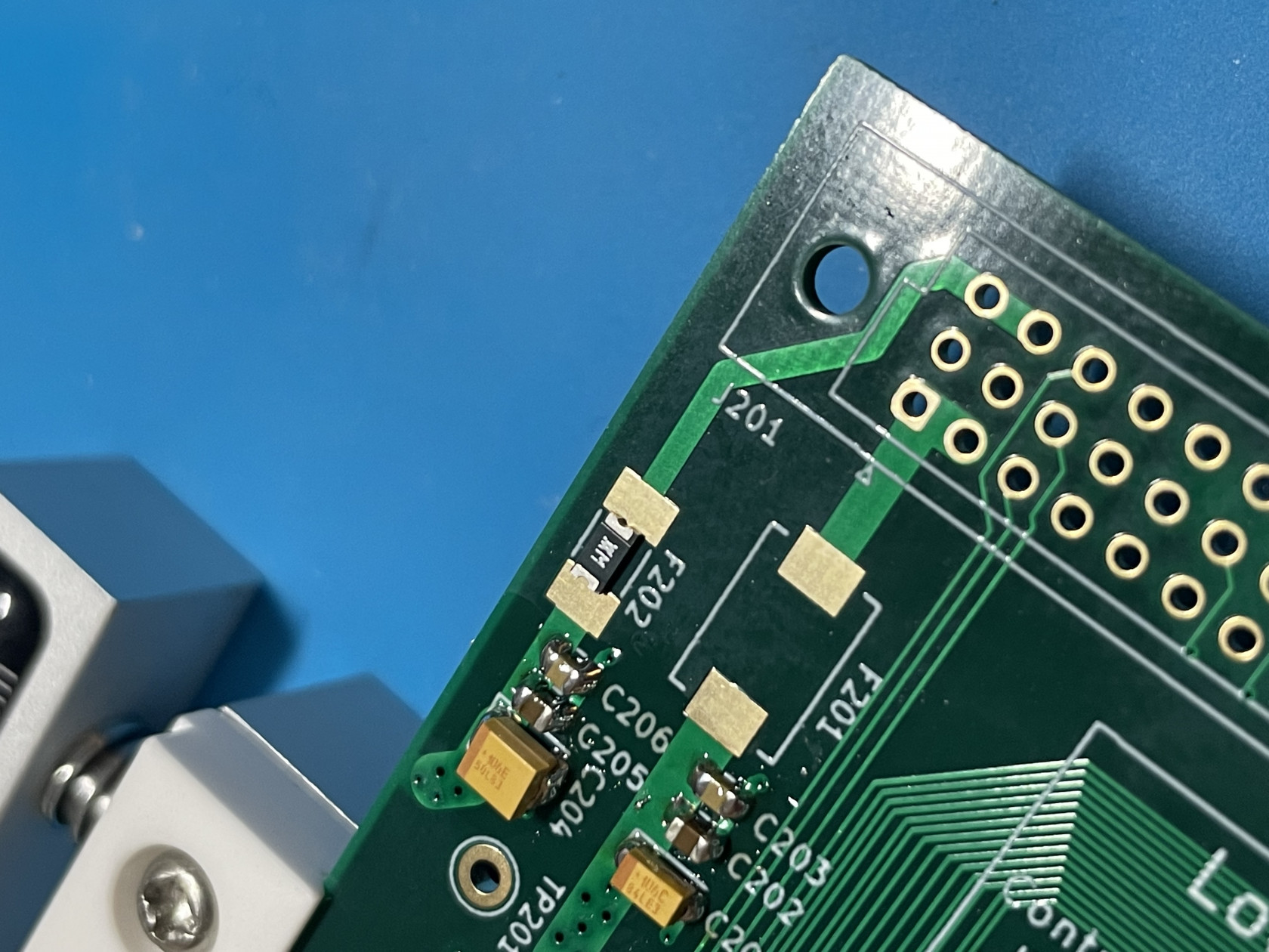](https://bookstack.trist.network/uploads/images/gallery/2021-12/5GJyDNp7dgQlSlo1-4c4b7710-7f08-4d19-beb5-0a50049fe9e9.jpeg)
- F201 is actually 1.1A, not 1.5A as the schematics indicate
- Caps under Teensy (C316/C317) could use with being moved a bit
- U508/U509 package sucks ass
- C512/C511 should be further away from IC in -Y
- The indications for RESET and HALT are inverted (D401, D402) from what they should be
- Teensy USB port interferes with J302 with some USB cables
- Solder pads for DIN connectors could be slightly wider copper
- Logic probe connectors need more spacing in Y direction to fit the probes
[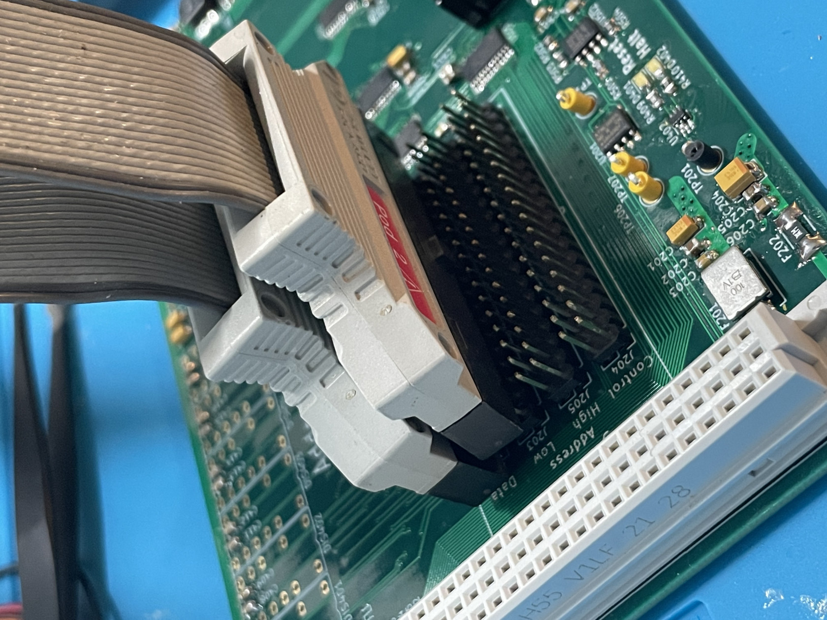](https://bookstack.trist.network/uploads/images/gallery/2021-12/KJWGCCiFa9ED0Yu9-d9eaace4-419b-4d2a-88fb-b2a40d43b003.jpeg)
### CPU Board
- +12V fuse (F202) footprint is wrong
- Reset and NMI button logic is inverted from what it should be (lol)
- U501 shouldn't be inverting type (use 74HC2G17 instead)
- D201 should be further set back (.3mm) from board edge
- The H100 series LED seems to have a slightly different pin-to-front distance than the H201 double LED indicators
- 5V Analog caps (C608, C609, C614) should be up more
- LED current limiting resistors are out of whack
- Lower the current limiting resistors for right angle LED indicators (needs more current)
- Increase the current limiting resistors for two bonus debug LEDs (needs less current)
- Read/modify/write cycles may not work right
- We need to deassert /DTACK when both /LDS and /UDS get deasserted
- Neither of the byte strobes are on U102, which is responsible for generating /DTACK
- *May* be able to bodge these into the GAL, since there’s a few spare inputs
- Also, the /BERR timer and peripheral waitstate generator are reset by /AS
- Probably a non issue since RAM is going to be 0 waitstate, and we can say CPU board peripherals don’t support read-modify-write (maybe only an issue for NVRAM)
- UART B (J503) should be centered between LEDs and UART A jack
# Backplane
Cards are interconnected via a simple backplane. Together with a management card, the backplane provides power, bus control signals, out of band signaling and support for per card audio outputs.
# Pinout
Using 96 position (3x32) DIN 41612 connectors; right angle male on expansion cards, vertical female on the backplane side. The management card uses a 48 position (3x16) DIN 41612 (C2) right angle male connector, with the corresponding vertical female on the backplane side.
## CPU Board
The pinout of the CPU board’s expansion connector is documented on the [CPU board expansion page.](https://bookstack.trist.network/books/68komputer/page/expansion "Expansion")
## Management Card
This provides power input to the rest of the backplane, and provides connectors for the mixed audio from the backplane.
| | **A** | **B** | **C** |
| **1** | +5V | +5V | +5V |
| **2** | +5V | +5V | +5V |
| **3** | +5V | +5V | +5V |
| **4** | GND | GND | GND |
| **5** | +12V | +12V | +12V |
| **6** | GND | GND | GND |
| **7** | | GND | |
| **8** | | GND | |
| **9** | | GND | |
| **10**
| | GND | |
| **11** | | GND | |
| **12** | /EXTRST | GND | |
| **13** | | GND | I2C\_IRQ |
| **14** | I2C\_SCL | GND | I2C\_SDA |
| **15** | | GND | |
| **16** | SNDR | GND | SNDL |
Any empty cells are not filled in are considered reserved for future use, and should be left unconnected.
#### Remarks
1. SNDL/SNDR refers to mixed audio from all cards (CPU + expansion) in the system.
2. EXTRST: when asserted, the CPU board (and with it, all peripherals on the backplane) are reset. This is equivalent to pushing the reset button on the CPU board, if it has one.
## Peripheral
These connectors are provided by peripherals; they're 96-position, 3 row type C DIN 41612 connectors. They shall be right angle, male type.
| | **A** | **B** | **C** |
| **1** | +5V | GND | +12V |
| **2** | +5V | GND | +12V |
| **3** | I2C\_SCL1 | /I2C\_IRQ1 | I2C\_SDA1 |
| **4** | GND | GND | GND |
| **5** | GND | D8 | D13 |
| **6** | D9 | D11 | D15 |
| **7** | D10 | D14 | D12 |
| **8** | D7 | D5 | GND |
| **9** | D6 | GND | D3 |
| **10**
| GND | D4 | D1 |
| **11** | D2 | D0 | GND |
| **12** | GND | GND | A22 |
| **13** | A23 | GND | A19 |
| **14** | GND | A21 | A17 |
| **15** | A20 | A15 | A18 |
| **16** | A13 | A16 | A12 |
| **17** | A14 | A10 | GND |
| **18** | A11 | GND | A8 |
| **19** | GND | A9 | A6 |
| **20** | A7 | A4 | A2 |
| **21** | A5 | A3 | A1 |
| **22** | R/W | /LDS | /UDS |
| **23** | GND | /DTACK | /AS |
| **24** | CLK | GND | |
| **25** | FC1 | FC0 | FC2 |
| **26** | | | |
| **27** | /IRQ\_IN | /DETECT | GND |
| **28** | /IRQ\_OUT | /BG | /HALT2 |
| **29** | /RESET2 | /BR2 | /BGACK2 |
| **30** | /IACK | /IRQ2 | /BERR2 |
| **31** | GND | GND | GND |
| **32** | SNDR | GND | SNDL |
#### Remarks
1. Pulled up to +5V by backplane
2. These signals should be driven as open drain; they're pulled up by either the backplane or CPU board.
3. If the card doesn't provide sound, tie SNDL/SNDR to ground through a 100kΩ resistor.
4. Cards should tie /DETECT to GND so that the backplane can detect which slots are occupied, even if the card doesn't have anything on its I2C bus.
#### Interrupt Arbitration
Peripheral cards arbitrate interrupt priority in slot order. This works by means of a daisy-chained interrupt request line from each slot to the next. The first slot has the daisy chain input tied permanently high. Each peripheral outputs whether it has a pending interrupt on these pins, and then asserts the shared interrupt line. When an interrupt acknowledge cycle takes place, the peripheral with the highest priority – that is, whichever has an `/IRQ_IN` that's deasserted – responds.
When its interrupt conditions are cleared (from within its ISR,) it will deassert `/IRQ_OUT` and `/IRQ`. If there's a lower priority card requiring attention, the interrupt will fire again and it will respond. Otherwise, the processor returns to normal execution.
The `/IRQ_IN` pin on cards is pulled down to GND with a 1MΩ resistor on the backplane for all slots to prevent erroneous interrupt behavior if cards aren't inserted one after another in the backplane, e.g. the interrupt priority chain is broken. Cards can drive these pins either directly, or open drain, but in the latter case, it must provide the required pull up resistors. For open drain driving, a pull up value of at least 47kΩ is suggested.
# 6 Slot Backplane
A backplane which supports up to six expansion cards, meant to go into a 3U VME crate.
[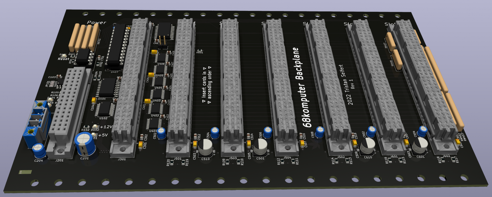](https://bookstack.trist.network/uploads/images/gallery/2022-02/tQs9sMlcRHkQvqGZ-image-1643962680396.png)
## Features
- Direction-controlled buffers for address and data bus
- Mixer for audio from CPU board and expansion slots
- Detection of installed peripheral cards via detect lines
- An I2C bus switch to allow CPU board independent access to each slot’s sideband bus
- Extremely low jitter clock distribution
It’s intended to be used in conjunction with the [backplane management](https://bookstack.trist.network/books/68komputer/page/management-card "Management Card") card for power, but the required +5V and +12V rails can also be provided through a 3.81mm pitch pluggable terminal block instead.
## Assembly Notes
Here are some notes about hardware revisions.
### Rev 1
- The ID EEPROM is an AT24CS16, which has a different protocol than the AT24CS32 specified in the schematic. The address pins are also "NC" there
- Drop resistors for orange/yellow LEDs (R401, R107, R108) should be a lower value
- R401 probably got assembled wrong
- Drop resistors for yellow LEDs (R101, R102) should be slightly higher
- Or, we just spec shittier green LEDs
- They're just slightly too bright
# Backplane Management
Provides +5V and +12V power and supervision for backplane, and audio output.
# Overview
Unlike other expansion boards, this one is required to operate the backplane, primarily to power the system. To connect, it uses a smaller half height (48 position, 3 row) DIN 41612 connector with a [unique pinout](https://bookstack.trist.network/books/68komputer/page/pinout "Pinout") to interface to the backplane. Additionally, it exposes mixed audio from all expansion sources with volume control.
[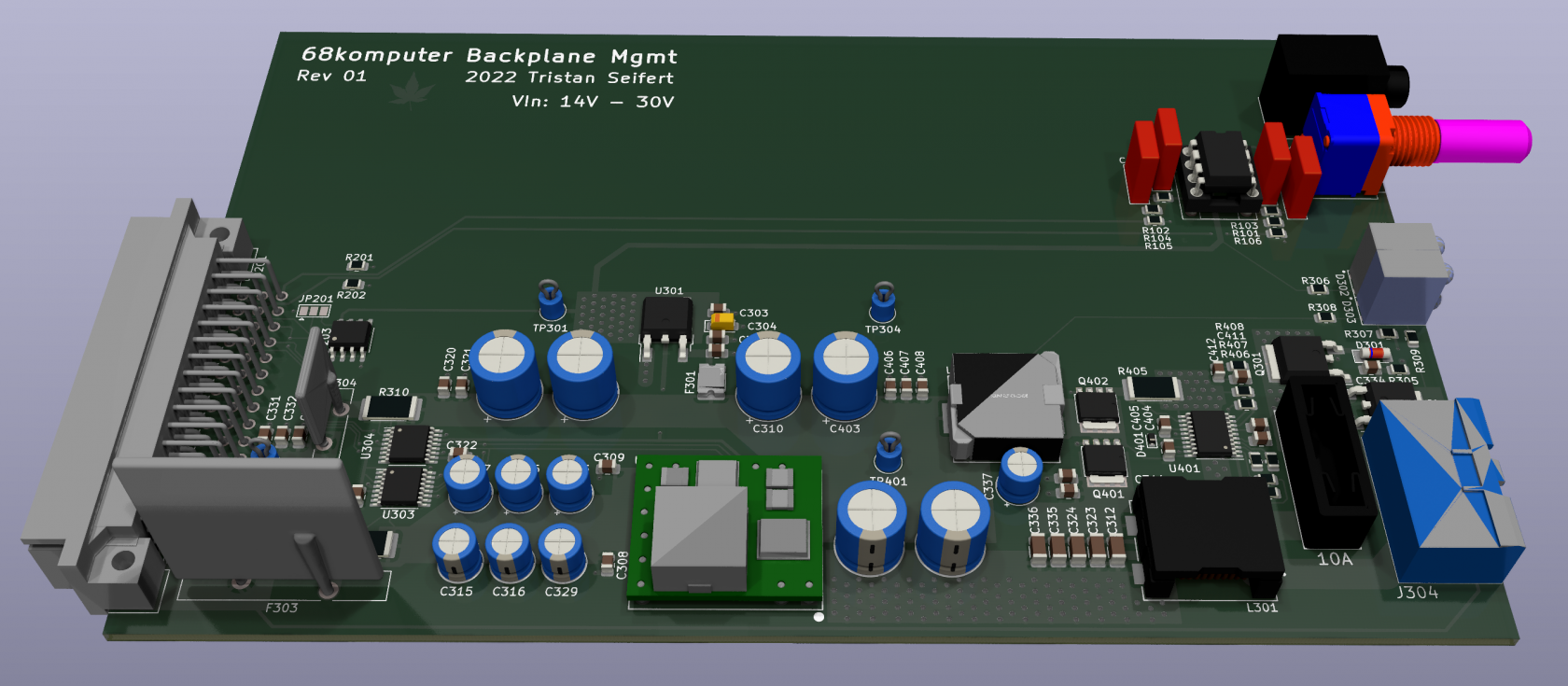](https://bookstack.trist.network/uploads/images/gallery/2022-02/4DJ7ymriRaR2WFvi-image-1643961820302.png)
Shown above is the Rev1 board backplane management board. This board is two layer, with 2oz copper.
## Power
Primarily, the management card exists to provide power to the rest of the system. It accepts any voltage between 14V – 30V through a pluggable 5.08mm pitch terminal block (CUI TBP01R1W-508, but compatible with many other pluggable terminal blocks) as an input. The input features reverse polarity protection and inrush current limiting, and a 10A replaceable fuse. Input power then passes through a common mode choke to filter out noise.
Next, the main +12V power rail is generated via a [LM25116](https://www.ti.com/product/LM25116) switching controller (U401) with discrete MOSFETs (Q401, Q402.) A maximum of roughly 10A at 12V can be supplied. The +12V rail then has significant bulk decoupling, since it provides both the system’s +12V rail, and the input for the other regulators.
The system’s +5V rail is generated by a [PTH08T220](https://www.ti.com/product/PTH08T220W) power module; it can provide up to 16A of power. A secondary +5V rail, used exclusively by the management board, is generated using a linear regulator (U301) from the +12V rail. The secondary rail powers the audio amplifier, as well as all active logic on the card.
Lastly, both the +5V and +12V rails pass through 3mΩ current shunts, which is measured by an [INA209](https://www.ti.com/product/INA209) current sense device (U303, U304.) These devices expose the voltage/current/power readings over the I2C bus, which can be read out by the host. (There’s also programmable upper/lower bounds and fault outputs, but these are not currently used.)
Both rails then have some further high frequency decoupling on the output, after the current shunt, followed by polyfuses: 13A on 5V, and 5A on 12V.
## Audio
Additionally, the card buffers the mixed audio signals provided by the backplane. The audio is filtered by an active low-pass filter with a 16kHz cut-off frequency. A stereo potentiometer is used to control the volume of the output audio, which is provided on a 3.5mm jack.
## Miscellaneous
Like all other expansion cards, the management card supports the I2C bus for out-of-band management, and provides a configuration EEPROM (U203; it has an embedded serial number) at addresses `0b1010000` and `0b1011000`.
Indicators are provided for all power rails.
# Revisions
This page lists any assembly remarks and issues with each revision of the board.
## Rev 1
- 5V power module (U302) sync input should be grounded, to use internal sync.[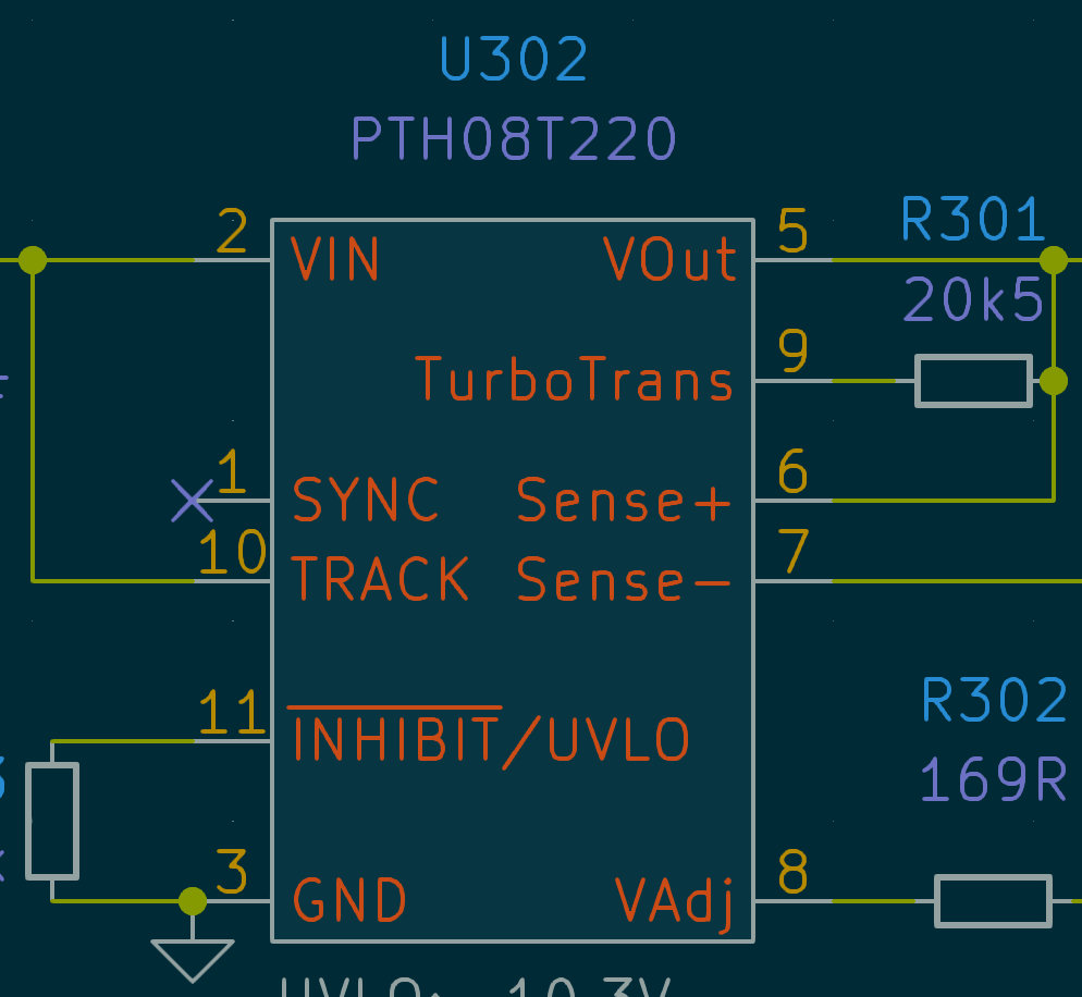](https://bookstack.trist.network/uploads/images/gallery/2022-02/KzY3FFoWXcskl9vp-image-1644815113713-46.png)
- Move capacitors out from under the 5V power module; it causes interference issues
- Annular rings on power module need to be wider (at least by .2mm;) they suck to solder to right now
- R201/R202 (100k pulldown on audio inputs) are redundant; they are already at the opamp (R105/R106)
- D401 sucks to hand solder (super tiny)
- Volume potentiometer RV101 should be logarithmic type